
Atoms:
Electrons of a single atom occupy a discrete set of energy levels. When measuring the energies of electrons in an isolated atom, we do not find a continuous distribution of energies, but a set of quantized energies.
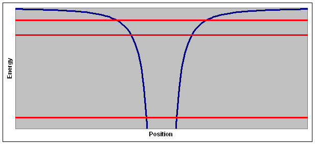
The plot above shows the potential energy of an electron and three possible values for the total energy. This model of discrete energy levels can also be extended to simple compound molecules, and experimental evidence can easily be found in the emission and absorption spectra of gases.
When atoms form a solid, the potential energy of each electron changes, and its possible energy values change. The energy of the more tightly bound electrons changes very little, and these electrons remain localized about a single atom. The less tightly bound electrons do not remain localized, and their possible energy values now fall into bands of allowed values separated by gaps.
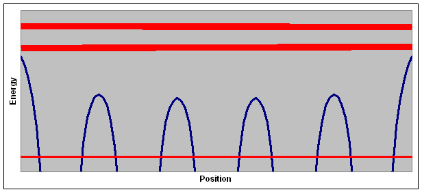
The plot above shows the potential energy of an electron, one possible energy for a localized electron, and two energy bands for delocalized electrons.
Consider a single atom of a particular species. This atom has a discrete set of energy levels. When another atom of the same species is brought close to the first atom, each of the energy levels becomes degenerate. But the interaction between the atoms breaks the degeneracy and the level splits into two separate energy levels. If this procedure is repeated >1020 times, each energy level will have split into >1020 level, effectively forming a continuous band of energy states.
Simulation: Quantum bound states
Although there may be an infinite number of bands in the band structure of a given material, there are two bands that are of particular significance in determining the electronic and optical properties of a material. These are the conduction band and the valence band. Note: These terms are defined below and may refer to the same band in materials that are conductors.
One of the most useful aspects of the band structure is the feature known as the band gap. In semiconductor and insulator materials, this usually refers to the gap between the valence band and the conduction band. The band gap and defect states created in the band gap by doping can be used to create devices such as solar cells, laser diodes, transistors, and a range of other electronic devices.
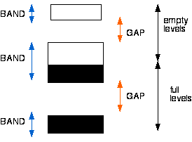
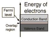
The properties of conductors, semiconductors and insulators are determined by the number of electrons that occupy the two highest lying energy bands that can hold electrons under normal circumstances. We therefore often only show these two bands in an energy level diagram. Each of the two bands can only accept a fixed number of electrons because it only contains a fixed number of states.
If all the states in a band are occupied, no net movement of electrons can occur and the band cannot contribute to the conduction of current. (All the wave functions of all the electrons interfere in such a way as to only form standing waves with zero average value for the momentum. We cannot build traveling wave packets.) An unoccupied band also does not contribute to the conduction of current.
It is easy to add a small amount of energy to some of the electrons, so
that they can move easily and conduct
electricity. But unless we apply a voltage electrons will move in
random directions, and no net current will flow. Electrons can
be accelerated by an electric field.
Even though an electric force is continuously acting on each electron when a
steady current is flowing in a wire, the electrons do not continue to
accelerate indefinitely, but reach an average terminal velocity, called the
drift velocity. When the electrons move with the drift velocity, then
the resistive forces (frictional forces) acting on them are equal in
magnitude and opposite in direction to the electric forces. Typical drift
speeds are on the order of 1mm/s.
The terminal velocity depends on the electric force and the resistive
force. The higher the terminal velocity, the larger is the current. The
current will increase if the voltage across the wire increases, (this
increases the strength of the electric field), and decrease if the resistive
forces increase in strength. Electrical conductivity is a measure of a
materials ability to conduct current.
The conductivity of good conductors decreases with
temperature.
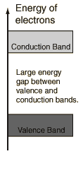
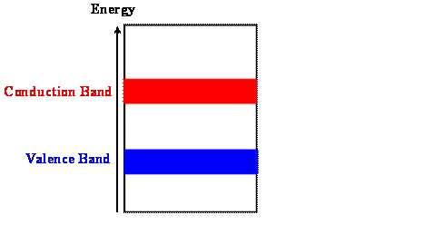
A large amount of energy is required to move electrons from the valence to
the conduction band. Only in the conduction band can electrons move
easily and conduct electricity. In insulators there are practically no
electrons in the conduction band. The amount of energy electrons can
gain from thermal agitation is not enough to lift them from the valence band
into the conduction band. The energy gap is too large. No
current can flow.
Problem:
What is the probability that an electron at the top of the highest filled
band will jump an energy gap of 3 eV to the conduction band at room temperature?
Solution:
The average number of fermions in a uniquely
defined quantum state with energy E is given by
PFermi-Dirac(E) = 1/(exp((E-EF)/kT) + 1).
With (E-EF) on the order of eV and kT = k*300K =
2.58*10-2 eV, we have exp((E-EF)/kT >> 1,
and the expression 1/(exp((E-EF)/kT) + 1) can be approximated by exp(-(E-EF)/kT.
The ratio of the average number of electrons in a state with energy E2
in the valence band to the average number of electrons in a state with
energy E1 in the conduction band therefore is
R = exp(-(E2-E1)/kT = exp(-(3 eV)/kT) = 4*10-51.
The probability that an electron will jump the gap is essentially zero.
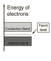
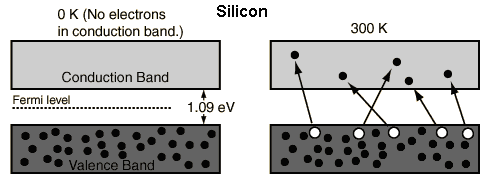
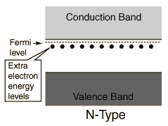
The properties of semiconductors lie between those of metals and insulators . For intrinsic semiconductors like silicon and germanium, the Fermi level is essentially halfway between the valence and conduction bands. Although no conduction occurs at 0 K, at higher temperatures a finite number of electrons can reach the conduction band and some current can flow when a voltage is applied. In doped semiconductors, extra energy levels are added.
The increase in conductivity with temperature can be modeled in terms of the Fermi function, which allows one to calculate the population of the conduction band.
Where does the energy come from to put electrons in conduction band ?
Simulation: Conductivity
Doping
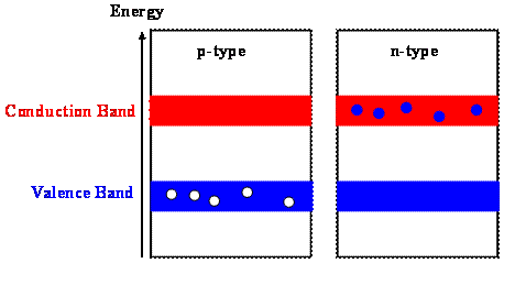
The addition of a small percentage typically (10-8% - 10-3%) of foreign atoms in the regular crystal lattice of silicon or germanium produces dramatic changes in their electrical properties, producing n-type and p-type semiconductors. Both silicon and germanium have 4 valence electrons per atom. Impurity atom with 5 valence electrons produce n-type semiconductors by contributing extra electrons.
Impurity atom with 3 valence electrons produce p-type semiconductors by leaving a deficiency and thus creating a hole.
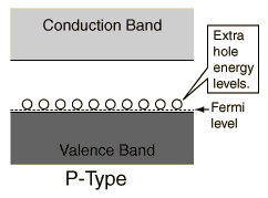
The addition of impurities in a p-type semiconductor creates some holes in the valence band. The addition of impurities in a n-type semiconductor puts some electrons in the conduction band. (The addition of impurities also changes the band structure slightly, but we ignore this in a simple model.) The holes in the valence band of the p-type material and the electrons in the conduction band of the n-type material can have net movement through the material and we call them free carriers. The doped material can conduct current.
p-n junctions
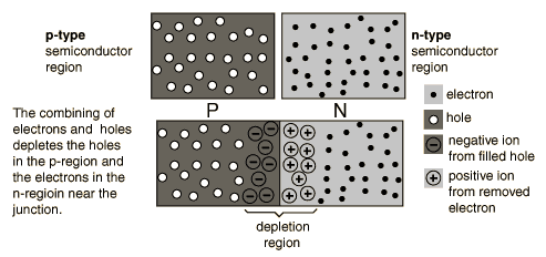
One of the crucial keys to solid state electronics is the nature of the P-N junction. When p-type and n-type materials are placed in contact with each other, the junction behaves very differently than either type of material alone. Specifically, current will flow readily in one direction (forward biased) but not in the other (reverse biased), creating the basic diode. This non-reversing behavior arises from the nature of the charge transport process in the two types of materials.
The open circles on the left side of the junction above represent "holes" or deficiencies of electrons in the lattice which can act like positive charge carriers. The solid circles on the right of the junction represent the available electrons from the n-type dopant. When a p-n junction is formed, some of the free electrons in the n-region diffuse across the junction and combine with holes to form negative ions. In so doing they leave behind positive ions at the donor impurity sites.
How does a voltage affect the energy levels?
Assume you established an electric field between the two semiconductors. Assume they are not in contact and no current flows.
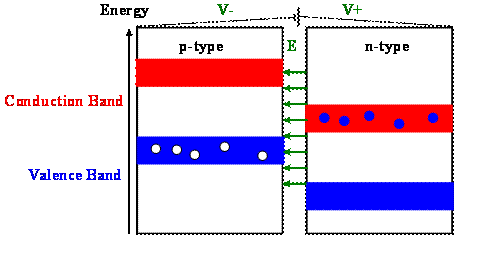
If the field points from the n-type to the p-type semiconductor, then the potential is higher in the n-type semiconductor, and the potential energy of the electrons is higher in the p-type semiconductor. (Electrons are negatively charged and their potential energy has the opposite sign as the potential.)
A p-n junction photodiode
The simple model presented here mixes a quantum mechanical with a classical description. Assume you bring a n-type and a p-type semiconductor in contact with each other.
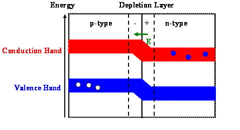
Electrons in the n-type semiconductor fill some of the holes in the p-type semiconductor because these holes are available lower-energy states. This leaves positively charged cores in the n-type and extra negatively charged electrons in the p-type semiconductor material. The n-type semiconductor becomes positively charged and the p-type semiconductor becomes negatively charged. A depletion layer free of mobile electrons and holes forms. An electric field points from the n-type to the p-type semiconductor in this depletion layer. This is equivalent to an applied voltage as in the previous figure. The energy bands in the p-type semiconductor move up and the energy bands in the n-type semiconductor move down. When the energy of the states in the conduction band of the n-type semiconductor is equal to the energy of the states in the valence band of the p-type semiconductor, lower lying energy states are no longer available for the electrons in the conduction band of the n-type semiconductor, and the filling of the holes stops.
Exposing the junction to light
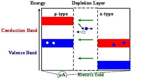
If a photon strikes the p-n junction and creates an free electron-hole pair in the depletion layer, then the electron will be accelerated towards the n-type and the hole towards the p-type side. If many photons create electron-hole pairs, a pico-ammeter connected across the junction will register the flow of a small current. This current crosses the junction from the n-type to the p-type material.
Reverse biasing the junction, i.e. connecting the positive terminal of an external power supply to the n-type side and the negative terminal to the p-type side will increase the size of the depletion layer. The external field will pull free electrons in the n-type material and and holes in the p-type material away from the junction.
An ordinary diode
An ordinary diode is forward biased. Connecting the positive terminal of an external power supply to the p-type side and the negative terminal to the n-type side prevents a shift of the energy levels due to the the buildup of negative charge on the p-type side and positive charge on the n-type side. The external field cancels the internal field, erasing the depletion layer. Recombination of electrons and holes can continue and a current will flow across the junction from the p-type to the n-type material.
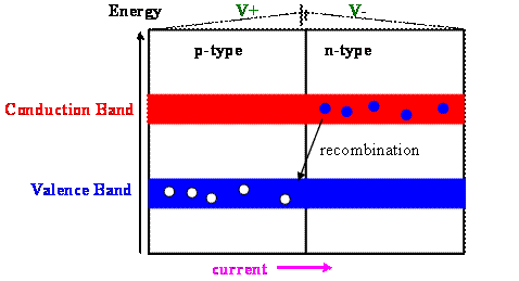
During the recombination energy is released. It can be released in the form of heat, or in the form of light, as in LED's and Laser diodes.
Problem:
An LED emits light with a wavelength of 500 nm. The LED is constructed from a p-n junction. What is the magnitude of the energy gap of the material?
Solution:
Assume the transitions are from the bottom
of the conduction band to the top of the valence band.
Then Egap = hf = hc/λ. Egap
= (4.136*10-15 eVs )*(3*108 m/s)/(500*10-9m)
= 2.48 eV.
Simulation: Semiconductors