
The goal of integrated optics (IO) is to develop miniaturized optical devices of high functionality on a common substrate. The state-of-the-art of integrated optics is still far behind its electronic counterpart. Today, only a few basic functions are commercially feasible. However, there exists a growing interest in the development of more and more complex integrated optical devices.
In IO we distinguish between optical integrated circuits, which perform functions similar to electronic circuits in communications systems, and planar optical devices, which are integrated optical systems other than communication systems.
![]()
Optical integrated circuits
Researchers hope to put wave guides, modulators, switches, and other active optical functions onto various substrates. It is visualized that thin films and micro-fabrication technologies can suitably be adopted to realize optical counterparts of integrated electronics for signal generation, modulation, switching, multiplexing and processing.
In optical integrated circuits, light is confined in thin film wave guides that are deposited on the surface or buried inside a substrate. Glasses, dielectric crystals and semiconductors can be used as substrate materials. The functions that can be realized depend on the type of substrate used. Researchers are challenged to identifying materials which have both the right electro-optical properties and a reliable means of forming them into useful structures on the integrated circuit. Unfortunately, many current-generation materials that are used to fabricate monolithic optical devices have high attenuation and therefore high transmission losses.
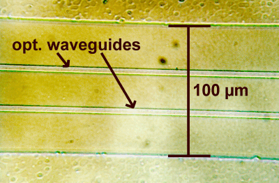
The most fundamental building block of an optical integrated circuits is a channel wave guide. Wave guides in integrated-optics work similar to conventional fibers, trapping light in a length of material. This material is surrounded by material of a different index of refraction. The wave guides are made either by depositing material on top of a substrate and etching unwanted portions away, or etching trenches in the substrate and filling them with polymers, silicates, or other light-transmitting materials.
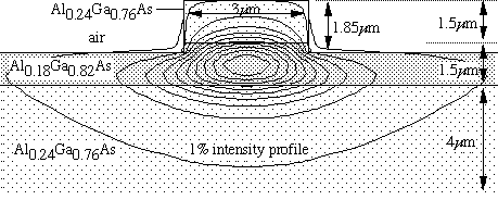
The basic requirements of a thin film optical guide material are that it be transparent to the wavelength of interest and that it have a refractive index higher than that of the medium in which it is embedded.
Within an optical integrated circuit, light propagates as a guided wave in a dielectric thin film. Appropriate addition of functional devices between interconnecting wave guides enables the realization of an optical integrated circuit for a specific use.
Some devices can be made on planar substrates using standard lithographic processes and thin-film technologies. Electron beam writing and laser beam writing are increasingly employed to produce patterns with high resolution. Epitaxial methods are used in the fabrication of sources, detectors and opto-electronic circuits on GaAs, Si and InP.
For a square channel wave guide of depth d the number of
modes is approximately m2, where m = (2d/λ)
NA, m >> 1. For a slab wave guide the number of modes is
approximately m. For single mode operation in any channel wave guide we
therefore need (2d/λ)*NA ≤
1, where d is the width of the channel. A single mode wave guide can be constructed by making d and NA
sufficiently small. NA is the
numerical
aperture and for small Δ is given by
NA = ncore(2Δ)1/2, where Δ = (ncore - ncladding)/ncore.
![]()
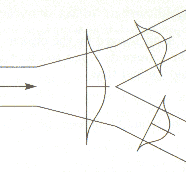
A branch in a wave guide consists of a single input wave guide, a short tapered section, and two output wave guides. Branches are used to divide a beam into many channels, but the loss at a branch is always significant. Cascading n branches results in a star coupler with 2n outputs.
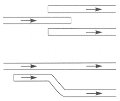
Directional couplers can be used as branches with less loss. Many directional couplers work by coupling the evanescent wave into the adjacent wave guide. The wave guides must be spaced approximately a wavelength apart. The wave that is excited in the second wave guide propagates in the same direction as the wave in the first guide. The spacing between the wave guides must be adjusted for the desired power transfer.
Another type of coupler is based on Bragg reflection. A fiber Bragg grating is made from a section of ordinary single-mode optical fiber, typically a few millimeters to a few centimeters in length. The grating is formed by causing periodic variations in the index of refraction of the glass lengthwise along the fiber. The period of the index modulation can be designed to cause deflection of light at a specific wavelength, the Bragg wavelength. Typically the light at the Bragg wavelength is selectively reflected while all other wavelengths are transmitted, essentially unperturbed by the presence of the grating.
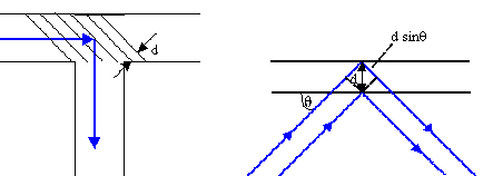
The condition for Bragg reflection is 2dsinθ = mλ', m = 1, 2, ..., where λ' = λfree/n is the wavelength of the light in the fiber. By combining fiber gratings in various arrangements, many different wavelengths can be separated and coupled out. A fiber Bragg grating's low-loss characteristics and its ability to selectively pass or reflect specific frequencies, make it a very versatile element that can be used in filters and de-multiplexers for wavelength division multiplexing networks.
Bragg reflectors can also be implemented in a channel wave guide. Diffraction gratings can be etched into the wave guide. The width of the channel compared to the wavelength of the light limits the number of grooves in the grating and therefore the finesse (the effective number of transmitted beams) of the grating. The more grooves a grating has, the sharper are the diffraction peaks.
For a grating the instrumental line width Δλ, or the wavelength difference between two peak that can just be resolved in mth order is Δλ = λ/mN, where N is the number of grooves. If a fiber or waveguide are used to transport signals at many different wavelengths, and these signals are supposed to be separated using a grating, the wavelength difference between two signals adjacent in wavelength must be greater than Δλ = λ/N.
![]()
A wave guide that splits into two equal-length sections which after a certain distance recombine becomes a Mach-Zehnder interferometer.
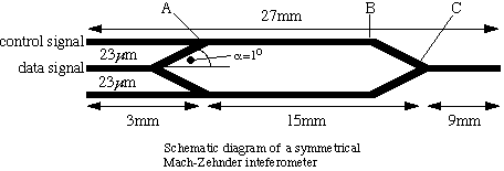
If the index of refraction of one of the path can be changed by applying some external signal, then, when the the two beams recombine, they can be made to interfere constructively or destructively in response to the external signal. Destructive interference can reduce the intensity of the resulting beam or turn it off completely. The interferometer therefore can be used as a switch.
Mechanically compressing some materials using a piezoelectric effect or an acoustic wave can change their index of refraction enough to accomplish the switching function. Some materials change their index of refraction in response to heat. A microscopic resistance heater or piezoelectric transducer in one leg of an interferometer made of such a material can be used to accomplish the switching function. However, switching speeds are low for acousto-optic (tens of microseconds) and thermo-optic (milliseconds) devices.
Some materials change their optical character in response to the application of an electrical signal. The current material of choice is lithium niobate (LiNbO3), which is a crystalline dielectric material with excellent electro-optical, acousto-optical and nonlinear optical properties. Mature technologies for the fabrication of optical wave guides in this material exist. The response speed of LiNbO3 devices is in the nanosecond range. The drawback of LiNbO3 is its high attenuation.
![]()
Examples of light-on-a-chip devices
|
Filters are used to select desired wavelengths out
of a wavelength division multiplexer (WDM) stream, or block a particular channel from being injected into
a multiplexer. | |
|
On/off switches can be created using many technologies, including Mach-Zehnder-effect devices. | |
|
Multiplexers/demultiplexers can be constructed for WDM applications to combine light from multiple sources, as well as extract a particular channel from a WDM beam. | |
|
Integrated optical amplifiers are replacing large spools of erbium-doped fiber that were pumped with laser energy to regenerate weak network signals. The most common integrated amplifier consist of a forward-biased heterojunction which carries current. It also contains a set of optical wave guides that confine the incoming signal to the junction's active region. These semiconductor optical amplifiers can be used simply for amplification, or tuned to provide frequency conversion. This ability to shift frequencies can be exploited to build many kinds of WDM switching architectures. |
The advantages of IO elements over their bulk optic counterparts are compact size, protection from thermal drift, moisture and vibration, low power requirements and low cost due to the possibility of batch fabrication.